In the electronics industry, “Form Factor” is everything. As devices become smaller, faster, and more powerful, the traditional methods of connecting components—wire bonding, soldering, and photolithography—are reaching their physical limits.
At this microscopic scale, a single micron of impedance or a minor thermal mismatch is a profound strategic liability (#77), threatening the Strategic Reliability (#19) of everything from a satellite’s radar system to a quantum computing array.
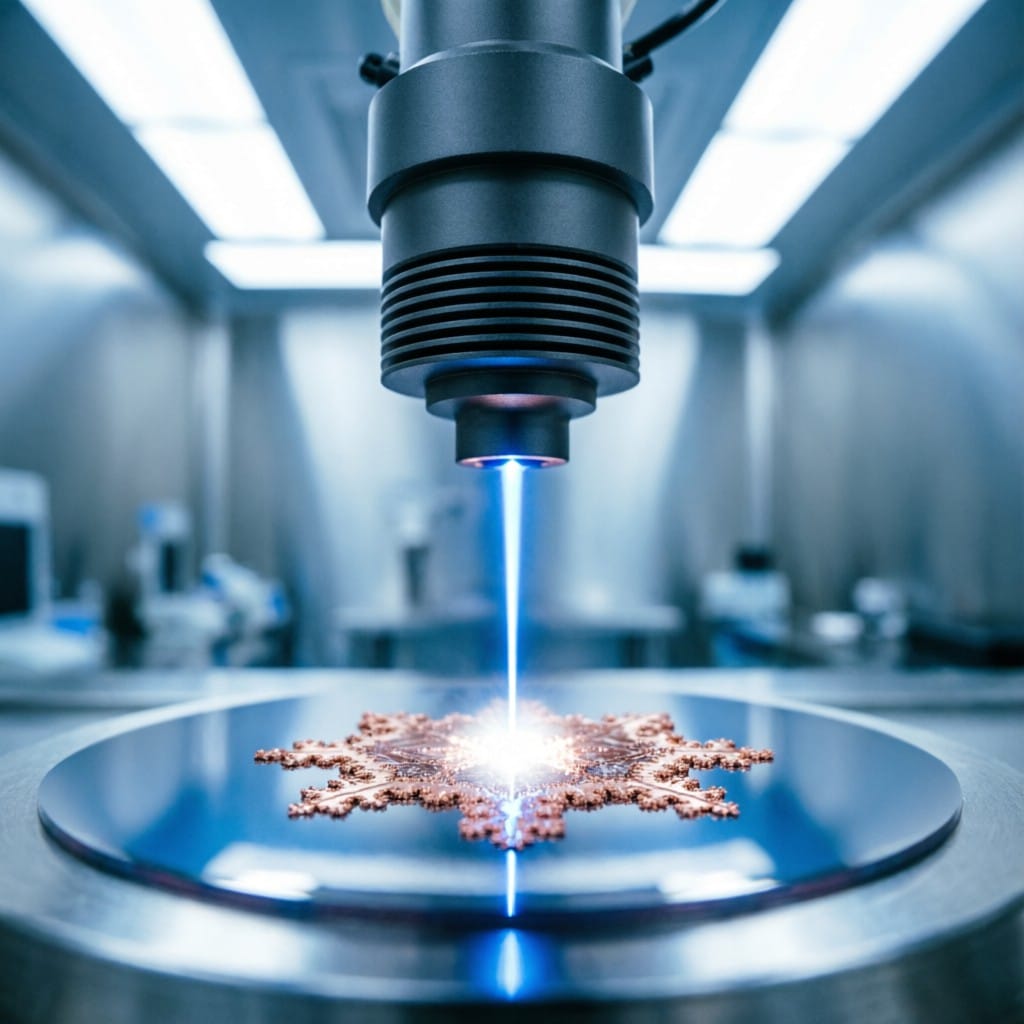
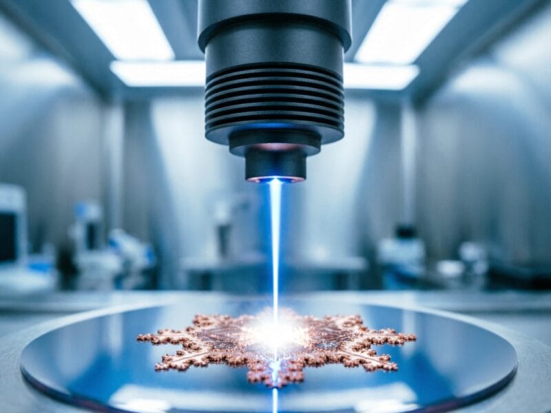
Intouchray (intouchray.com) is engineering the solution for this “Invisible Infrastructure.” By adapting Extreme High-Speed Laser Cladding (EHLA) (Article #33) protocols for micro-scale application, we are moving from “Depositing Material” to “Synthesizing Conductivity.”
We are proving that Noble Precision (#13) is the primary requirement for the future of Moore’s Law.
- Current Standard: Prototyping and Thermal Management
Today, Intouchray’s micro-cladding technology is deployed where standard additive processes fail. We are currently utilizing specialized EHLA heads (Article #27) for high-value prototyping in two critical areas:
Advanced Thermal Spreaders: As microprocessors generate more heat in smaller spaces, managing thermal flow is essential. We use micro-cladding to deposit ultra-thin layers of high-conductivity Metamaterials (Article #63), such as copper-diamond composites, directly onto silicon interposers.
This ensures that a component’s Digital Twin (Article #65) and physical performance remain synchronized, providing total Total Life-Cycle Sovereignty (Article #76).
High-Frequency Connectors: For 5G/6G and aerospace radar systems, current connectors create signal loss. Intouchray’s Current Noble Precision (#13) enables the prototyping of complex, 3D connectors with functionally graded metallurgy (Article #64), minimizing signal impedance and ensuring the Strategic Reliability of critical communications.
- The Investigative Frontier: Direct Logic Synthesis (Research Phase)
The ultimate goal of micro-cladding is the elimination of the distinction between “The Chip” and “The Package.” Looking toward our future roadmap, Intouchray is investigating Direct Logic Synthesis.
Micro-Deposition of Conductive Logic (Research Concept): We are exploring the use of femtosecond lasers (Article #27) and specialized micro-powders to directly deposit conductive traces onto active silicon, bypassing the entire photolithography step for specialized applications. This remains a concept for future direction.
3D Encapsulation (Research Concept): Our R&D team is investigating how to create functionally graded “shells” that provide integrated shielding against electromagnetic interference (EMI) and radiation, synthesized directly around a critical micro-component.
- The Digital Twin at the Micron Level
The success of micro-cladding relies on a fusion of metallurgy and data. At this scale, the distinction between the “Code” and the “Component” is dissolving.
Through the work with In-Situ Sensing (Article #34) and AI-driven synthesis (Article #66), every micro-cladded trace or thermal spreader is a data-verified artifact. This unparalleled level of verification is the hallmark of Total Life-Cycle Sovereignty (Article #76), ensuring that even at the micro-scale, Intouchray delivers an immutable standard of Zero-Defect quality.
Conclusion: Foundations of the Invisible
Article #86 proves that the “Quantum Beam” is the architect of the invisible world. We are building the foundations of the digital future, one micron at a time. In Article #87, we move from electronics to medicine: Biocompatible Bonds: Cladding for Advanced Medical Implants and Prosthetics.
Image Attachment